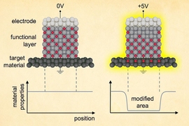
A new way of switching the magnetic properties of a material using just a small applied voltage, developed by researchers at MIT and collaborators elsewhere, could signal the beginning of a new family of materials with a variety of switchable properties, the researchers say.
The technique could ultimately be used to control properties other than magnetism, including reflectivity or thermal conductivity, they say. The first application of the new finding is likely to be a new kind of memory chip that requires no power to maintain data once it’s written, drastically lowering its overall power needs. This could be especially useful for mobile devices, where battery life is often a major limitation.
The findings were published this week in the journal Nature Materials by MIT doctoral student Uwe Bauer, associate professor Geoffrey Beach, and six other co-authors.
Beach, the Class of ’58 Associate Professor of Materials Science and Engineering, says the work is the culmination of Bauer’s PhD thesis research on voltage-programmable materials. The work could lead to a new kind of nonvolatile, ultralow-power memory chips, Beach says.
The concept of using an electrical signal to control a magnetic memory element is the subject of much research by chip manufacturers, Beach says. But the MIT-based team has made important strides in making the technique practical, he says.
The structure of these devices is similar to that of a capacitor, Beach explains, with two thin layers of conductive material separated by an insulating layer. The insulating layer is so thin that under certain conditions, electrons can tunnel right through it.
But unlike in a capacitor, the conductive layers in these low-power chips are magnetized. In the new device, one conductive layer has fixed magnetization, but the other can be toggled between two magnetic orientations by applying a voltage to it. When the magnetic orientations are aligned, it is easier for electrons to tunnel from one layer to the other; when they have opposite orientations, the device is more insulating. These states can be used to represent “zero” and “one.”
The work at MIT shows that it takes just a small voltage to flip the state of the device — which then retains its new state even after power is switched off. Conventional memory devices require a continuous source of power to maintain their state.
The MIT team was able to design a system in which voltage changes the magnetic properties 100 times more powerfully than other groups have been able to achieve; this strong change in magnetism makes possible the long-term stability of the new memory cells.
They achieved this by using an insulating layer made of an oxide material in which the applied voltage can rearrange the locations of the oxygen ions. They showed that the properties of the magnetic layer could be changed dramatically by moving the oxygen ions back and forth near the interface.
The team is now working to ramp up the speed at which these changes can be made to the memory elements. They have already reached rates of a megahertz (millions of times per second) in switching, but a fully competitive memory module will require further increase on the order of a hundredfold to a thousandfold, they say.
The team also found that the magnetic properties could be changed using a pulse of laser light that heats the oxide layer, helping the oxygen ions to move more easily. The laser beam used to alter the state of the material can scan across its surface, making changes as it goes.
The same techniques could be used to alter other properties of materials, Beach explains, such as reflectivity or thermal conductivity. Such properties can ordinarily be changed only through mechanical or chemical processing. “All these properties could come under electrical control, to be switched on and off, and even ‘written’ using a beam of light,” Beach says. This ability to make such changes on the fly essentially produces “an Etch-a-Sketch for material properties,” he says.The new findings “started as a fluke,” Beach says: Bauer was experimenting with the layered material, expecting to see standard temporary capacitive effects from an applied voltage. “But he turned off the voltage and it stayed that way,” with a reversed magnetic state, Beach says, leading to further investigation.
“I think this will have broad applications,” Beach says, adding that it uses methods and materials that are already standard in microchip manufacturing.
Eric Fullerton, a professor of nanoengineering at the University of California at San Diego who was not involved in this work, says it could have applications for new kinds of magnetic memory that could have "some unique advantages, such as low operating voltage, nonvolatility, scalability, and CMOS compatibility. ... What is exciting here is that you can reproducibly change the [magnetic state] by changing the oxidation state of the interface."
In addition to Bauer and Beach, the team included Lide Yao and Sebastiaan van Dijken of Aalto University in Finland and, at MIT, graduate students Aik Jun Tan, Parnika Agrawal, and Satoru Emori and professor of ceramics and electronic materials Harry Tuller. The work was supported by the National Science Foundation and Samsung.


