
The key to creating a material that would be ideal for converting solar energy to heat is tuning the material’s spectrum of absorption just right: It should absorb virtually all wavelengths of light that reach Earth’s surface from the sun — but not much of the rest of the spectrum, since that would increase the energy that is reradiated by the material, and thus lost to the conversion process.
Now researchers at MIT say they have accomplished the development of a material that comes very close to the “ideal” for solar absorption. The material is a two-dimensional metallic dielectric photonic crystal, and has the additional benefits of absorbing sunlight from a wide range of angles and withstanding extremely high temperatures. Perhaps most importantly, the material can also be made cheaply at large scales.
The creation of this material is described in a paper published in the journal Advanced Materials, co-authored by MIT postdoc Jeffrey Chou, professors Marin Soljacic, Nicholas Fang, Evelyn Wang, and Sang-Gook Kim, and five others.
The material works as part of a solar-thermophotovoltaic (STPV) device: The sunlight’s energy is first converted to heat, which then causes the material to glow, emitting light that can, in turn, be converted to an electric current.
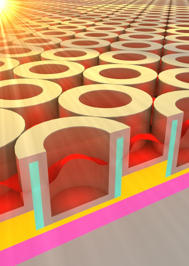
Some members of the team worked on an earlier STPV device that took the form of hollow cavities, explains Chou, of MIT’s Department of Mechanical Engineering, who is the paper’s lead author. “They were empty, there was air inside,” he says. “No one had tried putting a dielectric material inside, so we tried that and saw some interesting properties.”
When harnessing solar energy, “you want to trap it and keep it there,” Chou says; getting just the right spectrum of both absorption and emission is essential to efficient STPV performance.
Most of the sun’s energy reaches us within a specific band of wavelengths, Chou explains, ranging from the ultraviolet through visible light and into the near-infrared. “It’s a very specific window that you want to absorb in,” he says. “We built this structure, and found that it had a very good absorption spectrum, just what we wanted.”
In addition, the absorption characteristics can be controlled with great precision: The material is made from a collection of nanocavities, and “you can tune the absorption just by changing the size of the nanocavities,” Chou says.
Another key characteristic of the new material, Chou says, is that it is well matched to existing manufacturing technology. “This is the first-ever device of this kind that can be fabricated with a method based on current … techniques, which means it’s able to be manufactured on silicon wafer scales,” Chou says — up to 12 inches on a side. Earlier lab demonstrations of similar systems could only produce devices a few centimeters on a side with expensive metal substrates, so were not suitable for scaling up to commercial production, he says.
In order to take maximum advantage of systems that concentrate sunlight using mirrors, the material must be capable of surviving unscathed under very high temperatures, Chou says. The new material has already demonstrated that it can endure a temperature of 1,000 degrees Celsius (1,832 degrees Fahrenheit) for a period of 24 hours without severe degradation.
And since the new material can absorb sunlight efficiently from a wide range of angles, Chou says, “we don’t really need solar trackers” — which would add greatly to the complexity and expense of a solar power system.
“This is the first device that is able to do all these things at the same time,” Chou says. “It has all these ideal properties.”
While the team has demonstrated working devices using a formulation that includes a relatively expensive metal, ruthenium, “we’re very flexible about materials,” Chou says. “In theory, you could use any metal that can survive these high temperatures.”
“This work shows the potential of both photonic engineering and materials science to advance solar energy harvesting,” says Paul Braun, a professor of materials science and engineering at the University of Illinois at Urbana-Champaign, who was not involved in this research. “In this paper, the authors demonstrated, in a system designed to withstand high temperatures, the engineering of the optical properties of a potential solar thermophotovoltaic absorber to match the sun’s spectrum. Of course much work remains to realize a practical solar cell, however, the work here is one of the most important steps in that process.”
The group is now working to optimize the system with alternative metals. Chou expects the system could be developed into a commercially viable product within five years. He is working with Kim on applications from this project.
The team also included MIT research scientist Ivan Celanovic and former graduate students Yi Yeng, Yoonkyung Lee, Andrej Lenert, and Veronika Rinnerbauer. The work was supported by the Solid-State Solar Thermal Energy Conversion Center and the U.S. Department of Energy.


