


Materials known as conjugated polymers have been seen as very promising candidates for electronics applications, including capacitors, photodiodes, sensors, organic light-emitting diodes, and thermoelectric devices. But they’ve faced one major obstacle: Nobody has been able to explain just how electrical conduction worked in these materials, or to predict how they would behave when used in such devices.
Now researchers at MIT and Brookhaven National Laboratory have explained how electrical charge carriers move in these compounds, potentially opening up further research on such applications. A paper presenting the new findings is being published in the journal Advanced Materials.
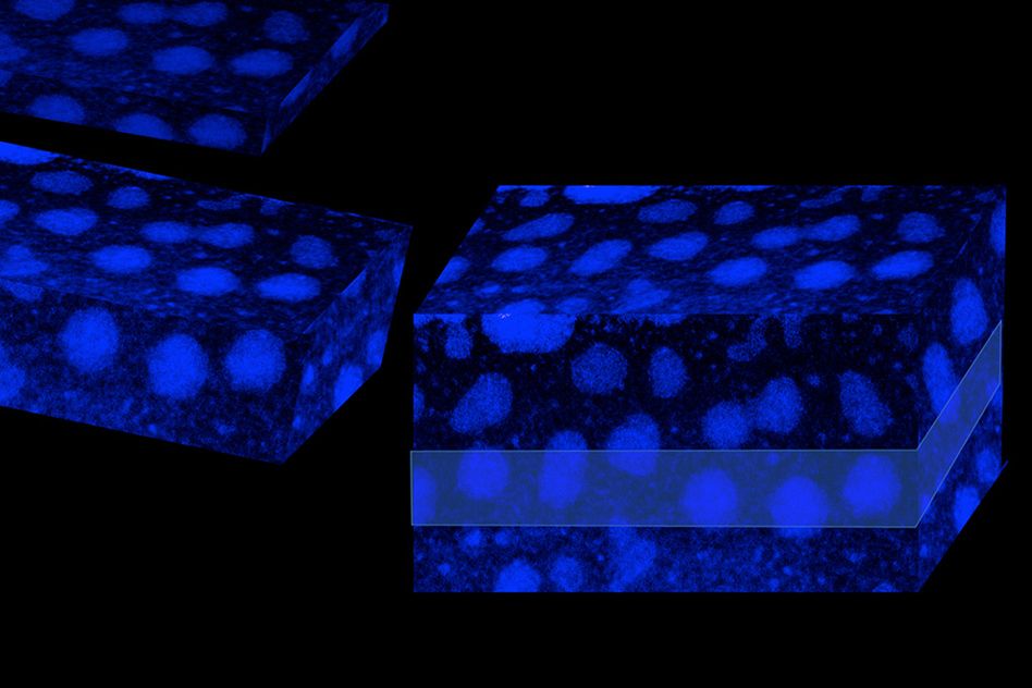
Conjugated polymers fall somewhere between crystalline and amorphous materials — and that’s caused some of the difficulty in explaining how they work, says Asli Ugur, an MIT postdoc and lead author of the paper. Crystals have a perfectly regular arrangement of atoms and molecules, while amorphous materials have a completely random arrangement. But conjugate polymers have some of both characteristics: regions of orderly arrangement, mixed randomly with regions of complete disorder.
“Some models have tried to explain how these materials behave, but there’s been no direct evidence,” Ugur says, for which model matches the reality. “Here, we’ve shown that the effect of crystallite size” —the sizes of the ordered domains within the material — plays a crucial role.
That’s because the trickiest part of conduction in such materials is what happens when charge carriers — in this case ions, or electrically charged atoms — reach the edge of one type of domain and have to “hop” into the next.
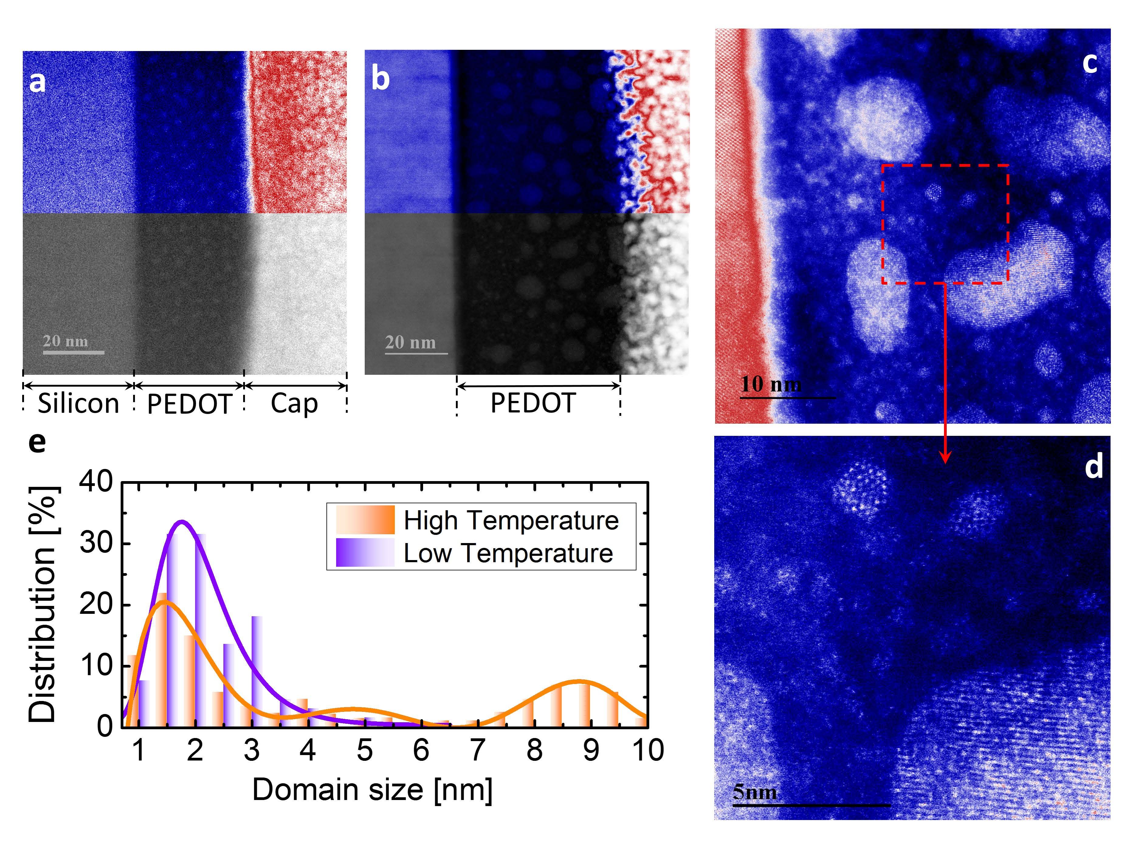
In bulk materials, those ions can go in any direction. But in this polymer, which can be very thin, there are fewer neighboring crystalline domains to which an ion can hop. With fewer options, conduction is more efficient, Ugur says, adding that, “As you get thinner, the conditions [for conduction] improve, even though the material didn’t change.”
Previous attempts to model the electrical behavior of such materials had focused on their chemical properties. “People didn’t take into account the crystallites,” says Karen Gleason, the Alexander and I. Michael Kasser Professor of Chemical Engineering. As a result, understanding of the electrical properties of such materials “remains incomplete even after decades of investigation,” the team writes in their paper.
Kripa Varanasi, an associate professor of mechanical engineering, says, “We wanted to develop materials where we can independently control their thermal and electrical properties. We were inspired to develop organic-inorganic interfaces as they can give rise to many new features that are not present in the corresponding bulk materials.”
Varanasi explains that most of the time, electrical and thermal conductivity of materials go together, but achieving independent tuning of thermal and charge transport can lead to broad applications for thermal management, flexible electronics and photonics, thermoelectrics, and thermal and electrical cloaking.
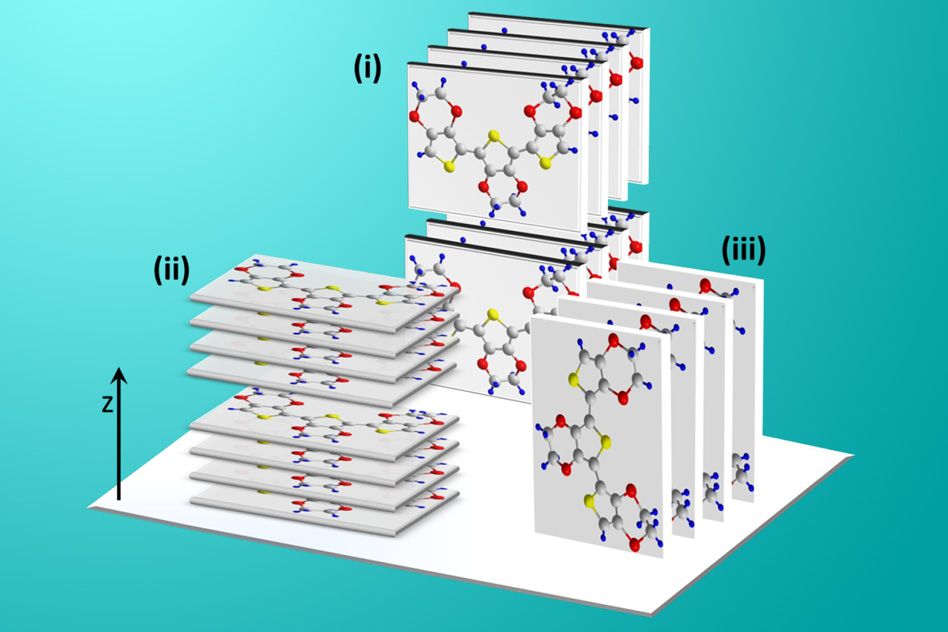
The researchers analyzed a conjugated polymer known as PEDOT, known to have a promising combination of good electrical conductivity and stability. One key question that this new research may help to answer, Gleason says, is: “What is the upper limit for conduction in this polymer?”
That’s information needed to assess its potential usefulness for various applications. When the material was first developed it had conductivity of between 1 and 10 Siemens per centimeter, or S/cm, Gleason says; over time, it was improved to a level of “close to 100.” Now, with the new analysis carried out by this team, conductivities of over 3,000 S/cm have been achieved. By creating ultrathin layers that amplify the hopping mechanism, “We are able to achieve ultraconductive, as well as highly transparent, films,” Varanasi says.
Other semiconducting materials used widely in electronics achieve even higher values, such as 8,000 S/cm in indium-tin-oxide, or ITO, Gleason says. But, she points out, those materials are stiff and brittle, whereas conjugated polymers are flexible, opening up potential applications in curved or flexible devices.
Although the research was conducted with PEDOT, Ugur says, the findings “should be generalizable to all conjugated polymers.” (Polymers’ structures consist of long chains; conjugated polymers are those that have at least one “backbone” consisting of alternating double and single chemical bonds, making them conductive).
PEDOT has a combination of three properties that give it great potential, Gleason says: electrical conductivity, transparency, and flexibility. “Anywhere that ITO is used, you could think of using this” — with added flexibility. The polymer material could have applications in flexible solar cells, displays, and touch screens, the team says, among other possibilities.
“This work is a significant step in the development and understanding of conductive polymer films,” says Ruud Schropp, a professor of thin-film photovoltaics at the Eindhoven University of Technology in the Netherlands, who was not involved in this work. He adds that the finding “explains the counterintuitive effect that ungrafted, amorphous PEDOT films have higher conductivity than grafted films. This insight could provide an avenue for bringing the conductivity of polymer films close to that of their transparent oxide counterparts, such as ITO.”
The research team also included MIT postdoc Ferhat Katmis and graduate student Mingda Li, and Brookhaven National Laboratory research scientists Lijun Wu and Yimei Zhu. The work was supported by the MIT Institute for Soldier Nanotechnologies, under contract from the U.S. Army Research Office, and by the U.S. Department of Energy.


